The TRS-20 - system bus
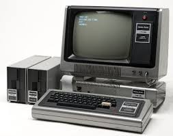
This project is influenced by Quinn Dunki’s 6502 homebrew machine Veronica, and a little by Radical Brad’s 74-series logic based Vulcan-74. Along with these two are a large number of existing homebrew computer builds, whose details provide me with a wealth of information on design ideas and likely problems I will face. There are even several kits available for order that solve a number of those problems for you.
Nevertheless, I will strike out on my own with a unique design, starting with the system bus.
This project has no purpose beyond its own journey. I have a computer already, so I don’t need to build one to get any work done. My computer is powerful enough to emulate an 8-bit 2MHz machine a dozen times simultaneously, so I don’t need to build one just to run some old software. Instead, the reason for this project is to connect at a more fundamental level with what a computer is, and how it works. Using a kit doesn’t achieve this - my understanding would remain theoretical, skipping over the hands-on experience of trying to get a bunch of ICs to come together as a working system.
Flimsy justification out of the way, let’s talk system bus design.
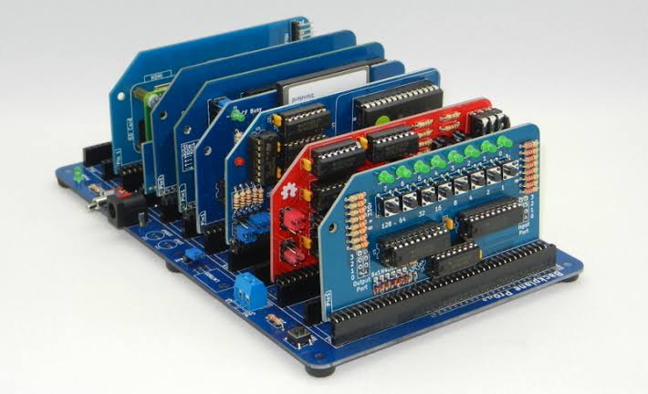
My experience with assembling PCs has exposed me to a common design pattern - a motherboard into which expansion cards are slotted. A variation on this pattern is used by the RC2014 system, by the Veronica, and by the Z50, amongst others. Rather than a motherboard carrying the CPU and core system components, though, these systems all have an uncomplicated parallel bus backplane board, and the CPU plugs in just like all the peripheral cards. This is a sensible choice, as the bus can be kept stable even if the CPU board iterates - or even changes processor entirely.
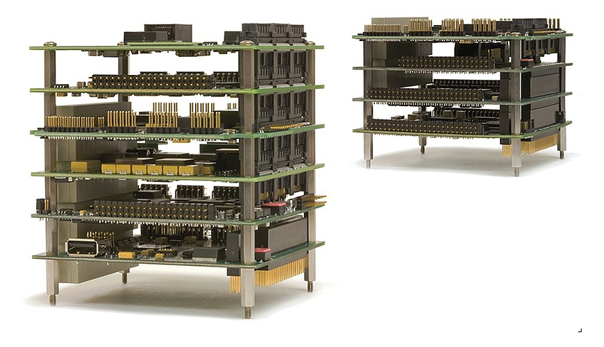
The RC2014, the Z50, and the Veronica are all motherboard designs with daughterboards rising vertically. They vary in the connector technology and pin count, but not widely. None of them are very well suited to my constraints on board size and my use of a Z180. 40-pin headers are slightly over 100mm long, exceeding my board budget. Trimming them takes an already heavily constrained signal set (down from 65 exposed on the Z180) and worsens the situation. ISA edge connectors are more suitable and remain a viable option, though 62 contacts means I’d need to skip three CPU signals and have no spare capacity for any other signals.
The winning choice, in the end, comes from a 30 year old standard for embedded systems. PC/104 is a vertical stack of small boards, using board to board connectors to run a bus, and standoffs to provide stability. Each board should be 90.17x95.89mm in size, with a 13mm allowance for I/O connectors at some edges, allowing me to use most of my board budget.
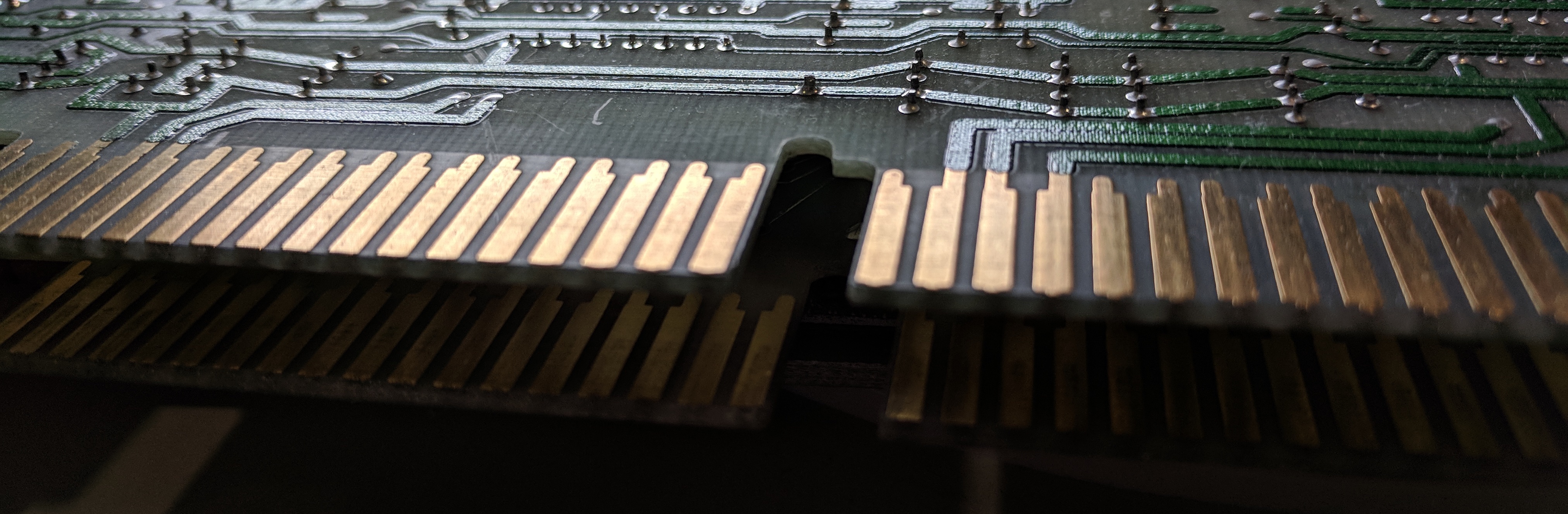
The original PC/104 bus was an ISA 8-bit (PC/XT) bus, with a 32x2 2.54mm pitch header for the board to board connections. This was subsequently updated to add a 20x2 header for a 16-bit ISA (PC/AT) bus. The original ISA bus uses edge connectors, not pin headers. The use of headers reduces the size of the bus connector down to fit on the PC/104 footprint. Subsequent revisions add a 4x30 header to carry a PCI bus, remove the ISA bus, add a PCI Express bus, and finally remove the PCI bus. These various kinds of bus connector are visible in the image above, but I’ll be sticking to the 16-bit ISA connectors - these are the headers included in my first round of parts.
It remains to be see whether I’ll actually use the ISA bus signals as they’re meant to be used. There isn’t exactly a real ISA bus specification, but the book “ISA and EISA: Theory and Operation” is about as close as it gets. There’s a few parts of correct ISA operation that might cause problems for my project. The ISA bus should be clocked at either 8MHz or 8.33MHz, though it’s reasonable to share the CPU clock. The clock isn’t particularly critical though, since the bus is asynchronous, with expected response times for each signal edge. There’s enough in common with the Z80’s system bus that a bridge should be practical to build, but it may have implications for whether I can get zero wait-state memory on the bus. To be determined…
I’m pleased with the notion of the PC/104 form factor. However, if it doesn’t work out as I’d like, I will fall back on more typical edge connectors. Five 2.54mm pitch 72-pin edge connectors is less than $15, and less than 100mm across (89mm for the pins, plus room for the edge of the header). PCI connectors have 120 pins, and at 1.27mm pitch are a comfortable 90mm or so for the whole connector, and cost about the same.
Meanwhile, because I’d like QFP parts to be an option I’ve also spent $5.84 on SMD soldering practice boards. The boards come with two QFP-44 chips each, some SOICs, a handful of resistors from 0402 up to 0805, some SOT23 chips, and some 0606 resistor arrays. Using SMD means more available parts, lower costs, and more effective use of my rather limited board space - but poking things with a hot metal stick might not cut it for much longer.
| Budget | CPU | Power | Keyboard | Video | Memory | Debug |
|---|---|---|---|---|---|---|
| $54.03 of $400 | █─── | ──── | ──── | ──── | ──── | █─── |