The TRS-20 - apply power here

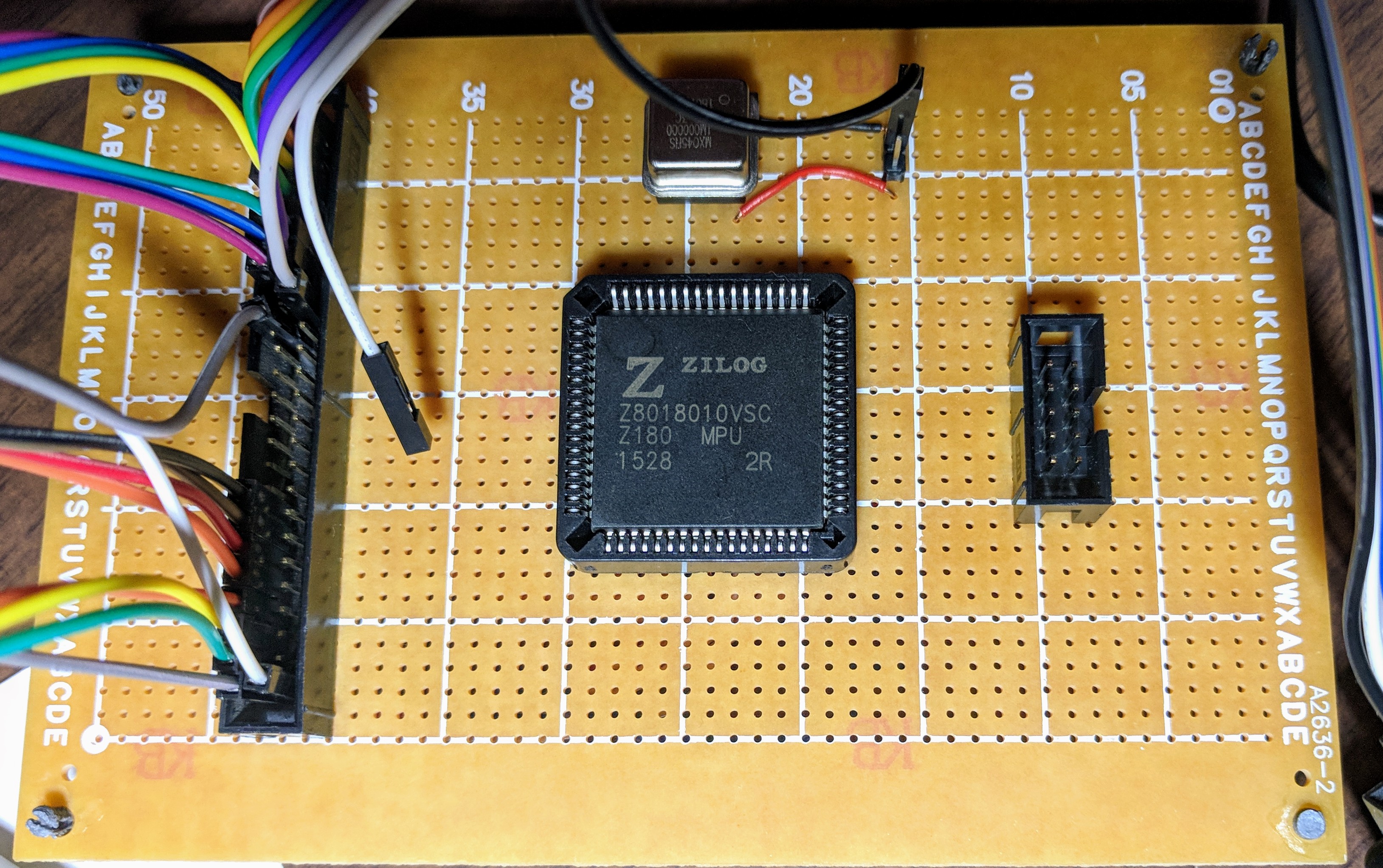
With my plan for a perfboard in hand, I finally broke out the soldering iron and started assembling. The board has a socket for an oscillator, a socket for the CPU, and IDC connectors for both 50-pin and 10-pin links. This is a lot of little wires to cut, strip, and solder. Let’s see how it goes.
Data, address, and more
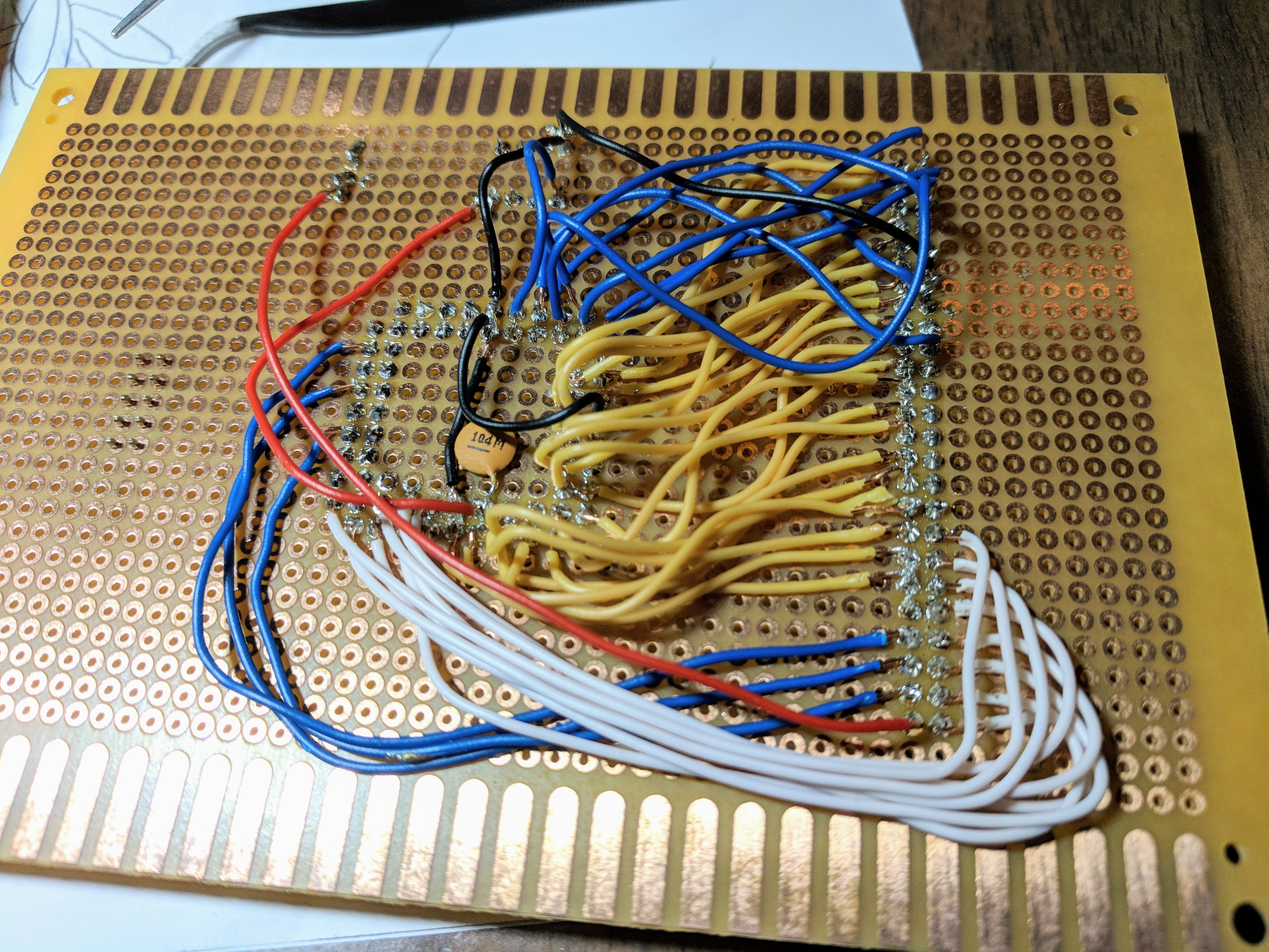
The first pass at it all involved 8 white wires for data, 16 yellow wires for address, some black and red for power lines, and not quite enough blue left for all the signals. There’s a capacitor that snuck its way on the board, since it’ll be noisy enough as it is. The soldering went as well as one might expect, you can see a few wires where the insulation has melted apart, a few suspiciously large blobs of solder, but everything’s clean and bridge-free.
The set of signals I chose to hook up with the blue I had are the CPU’s inputs: the four interrupts, reset, wait, and bus request. Wiring these seven signals high, and the eight data signals low, will put the CPU into a NOP loop through the low 8 bits of address space.
Using my ghetto fixed logic probe, the main thing I see is a smattering of chaos. The CPU has not been told otherwise, and so it is refreshing DRAM it doesn’t have. Each DRAM refresh sets some address lines and leaves others floating. The result on the probe is that I can find spans in which the low order address lines show a satisfying binary counting pattern, but the high order lines barely show structure at all.
Wiring up the rest
That’s okay. It’s time to wire up the remaining signals anyway. A quick trip to the local Jaycar (shout out to the Jaycar Aspley folks who’re super helpful every time I come in!) and I’m $9 down, but two packs of jumper wire up, and I can finish off the soldering. Except for the USART stuff to the 10-pin header, which I’ll leave for when I need it.
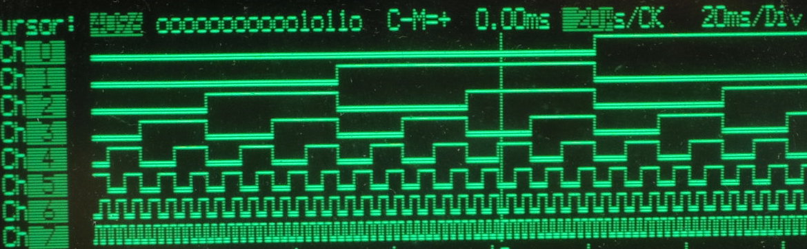
This time around, I’ll want to see what’s going on with the CPU status pins. I know that it should only be doing opcode fetches and refreshes, which means M1, MREQ, and RD are the only interesting signals. Connecting four pins of the probe to A0 through A3, and the other four pins to M1, MREQ, RD, and PHI lets me take a peek at what’s going on.
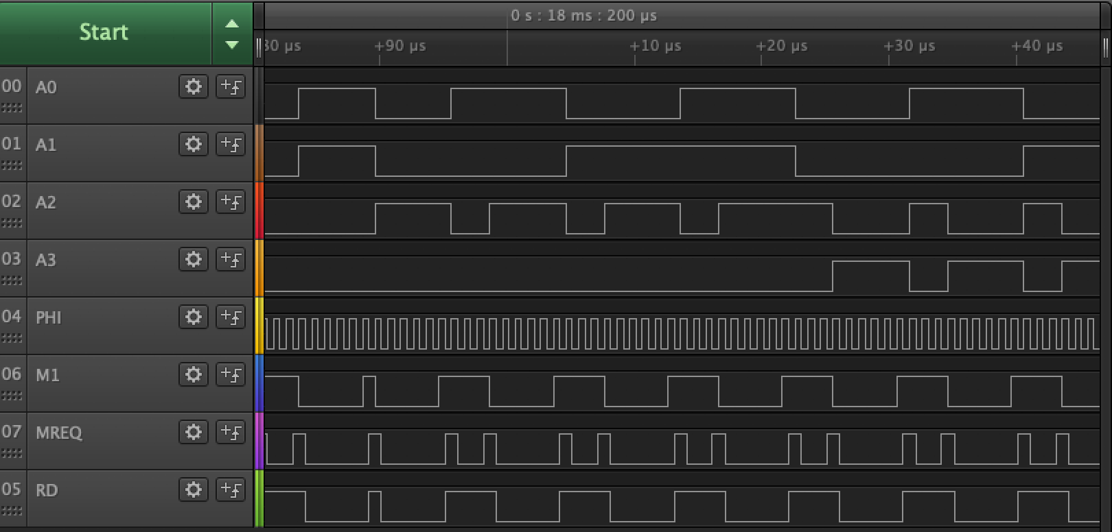
This image shows exactly what I expect. When M1 and RD are high but MREQ is low, the CPU is in a refresh cycle. The address lines will make some sort of sense, but not the sense I’m looking for. When M1. RD, and MREQ are all low, the CPU is fetching an opcode. The address lines are behaving as they should at these times.
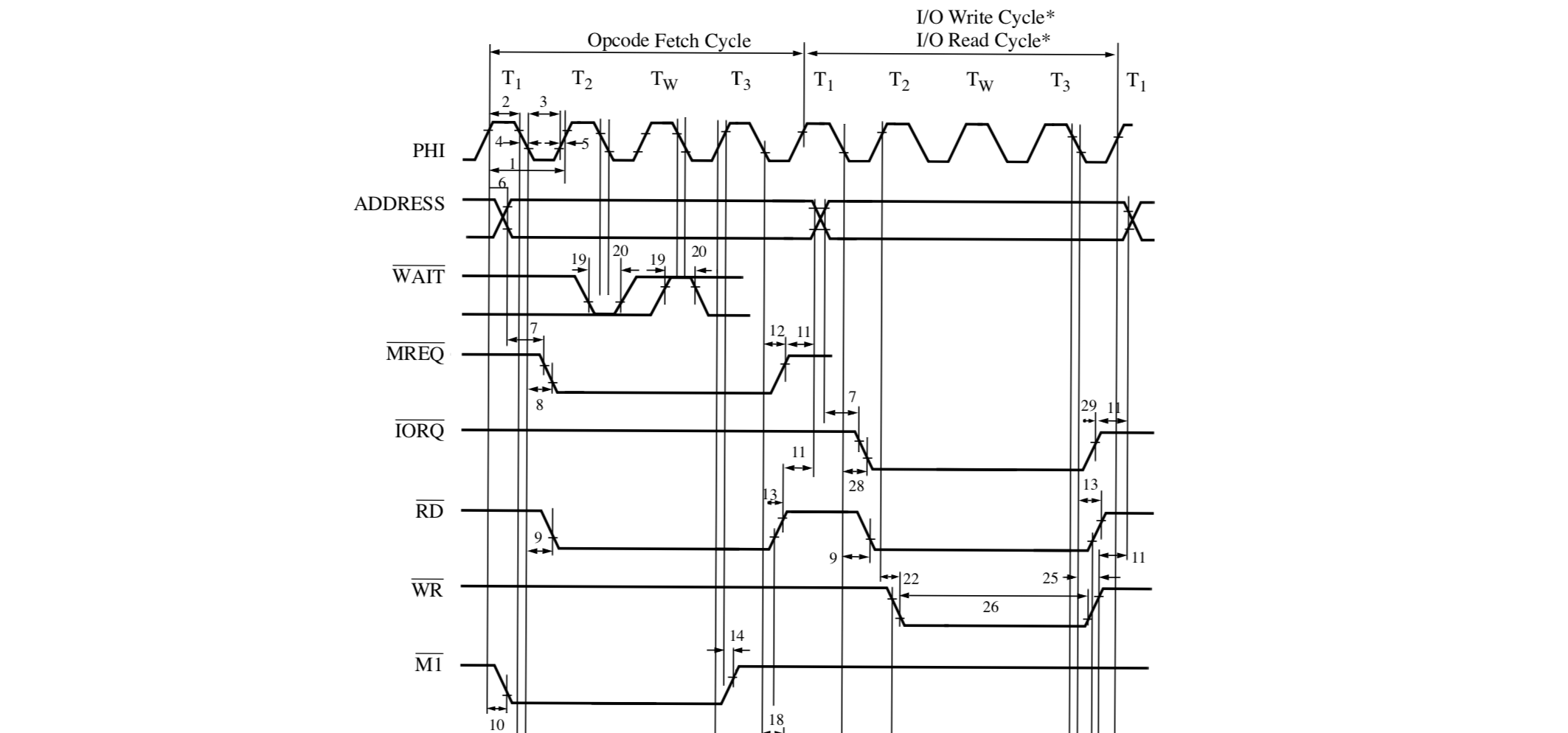
The synchronisation of signals matches the data sheet. Very shortly after Ф rises for T1, M1 falls. So shortly, in fact, my cheap logic probe records them as happening simultaneously, which means they are less than 41.7ns apart. At 10MHz, the data sheet promises these two events happen no slower than 60ns apart, and that looks to hold true at 1MHz as well. T1’s falling edge MREQ and RD both falling, no more than 50ns after. These three events coincide at a finer resolution than my probe. With T3’s rise, M1 rises. With T3’s fall, MREQ and RD rise.
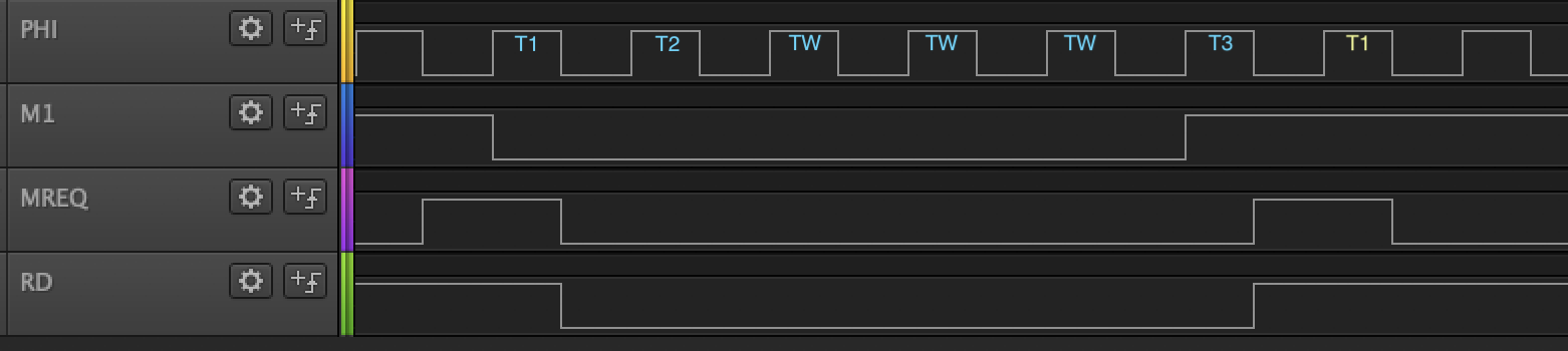
Since the CPU is only executing NOP instructions, all registers are at their RESET defaults. This includes the DMA/WAIT Control (DCNTL) register, which sets bits MWI0 and MWI1 at RESET, inserting three wait states to memory access cycles. The Refresh Control (RCR) register is also in its RESET state, which enables DRAM refresh, inserts one wait state in the refresh cycle to take it to three clocks, and requires one refresh cycle every 10 clock cycles. In practice, this means that there’s a memory refresh cycle between almost every opcode fetch cycle - every 7th fetch cycle skips a refresh cycle. In the image above, you can see a refresh cycle beginning. M1 and RD are high, MREQ is low.
The Z8018x Family MPU User Manual (UM005004-0918) has a table on page 287 that indicates a memory refresh cycle has M1, IORQ, RD, WR, HALT, and BUSACK high, and has MREQ and RFSH low. No other operating modes have MREQ active without either RD or WR active, that is . I don’t need to expose the RFSH line to know when a refresh cycle is active, and my boot ROM will disable memory refresh very early on in any case, so there’s no need to expose this signal.
One oddity does stand out. The system clock on PHI is running at 1MHz, the same as the oscillator. However, the Z8018x User Manual claims that “[T]he frequency of this output is equal to one-half that of the crystal or input clock frequency.” (UM005004-0918, pp. 7) This same claim is repeated in the Z80180 MPU Product Specification (PS014005-0817, pp. 9) for the CLOCK signal. This isn’t a problem, exactly, save that I have an 18MHz oscillator on back order, and that’ll be far too fast for my 10MHz rated chip.
Nevertheless, my chip starts up and looks on the surface to be behaving correctly. And perhaps more surprisingly, my soldering looks to have been done correctly!
Spending is a habit
| Item | Price | Purpose |
|---|---|---|
| SM1024 | $2.40 | 8-way DIP switch |
| WH3009 | $24.95 | 8 spools of 25m hookup wire |
| PB8819 | $9.95 | Breadboard w/ power supply and jumpers |
| RC5360 | $1.60 | 10x 100nF ceramic cap, through hole |
| RR0596 | $1.65 | 24x 10kΩ ±1% 0.5W resistor |
| PP1116 | $0.95 | 1x 50-pin IDC header |
| PP1100 | $1.90 | 2x 10-pin IDC header |
| HP9540 | $4.50 | Stripboard, 95x75mm |
| WH3032 | $9.00 | 2x breadboard jumper wire |
I picked up 8 spools of hookup wire. It’s wider than the jumper wire, and multi-core, so I haven’t used any yet. It’s great stuff for crimping into connectors and the like, but not so fun for soldering with - I expect it to last for years, but probably not see much use on this project. Towards the end of my $400 budget I will sort out what’s been used on the project and what hasn’t, so I can assess costs better.
The ceramic caps are handy for decoupling ICs: you can see one embedded in the processor board. The resistors are for pulling signals high or low. One 50-pin IDC header is now attached to a small section of stripboard, with male headers soldered beneath, as an IDC-to-DIP connector. It’s tricky, soldering to both sides of one-sided stripboard. The DIP switch was bought with dreams of toggling data lines high or low, but I’m not sure I’ll ever want to do that.
My PC104 stackable headers have failed to clear customs. I’ve received a refund, though sadly it looks like my refund doesn’t include the GST I paid for, so I’m out a dollar or so out of pocket, and I’ll need to re-order them sooner or later. Also from Aliexpress, I bought the logic probe from the last post for $12.93, but forgot to list it in any post, and have since also bought a MAX II CPLD minimum system board for $11.56 so I can experiment with a CPLD without soldering a hundred little wires, and some brass spacers for $5.20 for the PC/104 stack.
I think I can claim an extra mark on the CPU progress meter, since I have a working CPU.
| Budget | CPU | Power | Keyboard | Video | Memory | Debug |
|---|---|---|---|---|---|---|
| $209.35 of $400 | ██── | ──── | ──── | ──── | ──── | ██── |