
The TRS-20 - STM32F4 driver
With my plan sorted out, it’s time to get down to code. I’ll set up my build environment, take a look at testing options, configure timers, make a bunch of mistakes, and eventually test my hypothesis that an STM32F4 is fast enough to pretend to be the RAM and ROM for a 1MHz Z180.
Build first
I find it to be good practice for any project to start with the build and deployment processes. I want to be able to evolve my processes as my project evolves, and I don’t want to encounter infrastructure surprises late in the project when everything is more complicated and change is costlier.
My initial build process was a straightforward Makefile to build a single assembly source file with a single .text section and link it as per the Cortex M0 example I mentioned in the last post. This got me far enough to inspect binary outputs, which leads to understanding why my assembly sources should begin with the following three directives.
        .thumb
        .cpu            cortex-m4
        .unified
The STM32F series is based on a Cortex M4 design. The M4 permits two instruction sets, the ARMv7 and Thumb sets - the Thumb set has 32-bit extensions (sometimes called Thumb v2), and the STM32F4 only supports Thumb mode. The directives then tell the assembler to emit Thumb opcodes, to use the set of opcodes supported by the M4, and to use a unified syntax common to both sets as the original Thumb mnemonics kind of sucked.
Switching between ARMv7 and Thumb modes is accomplished with a couple of branch-and-exchange-mode instructions. If the target address has its least significant bit set, then Thumb mode is enabled. Otherwise, ARMv7 mode is enabled. I’ll never use the bx instructions, but this LSB signal also crops up for the processor’s vector table.
You could simply set the LSB on each address in the vector table with something like .word _start + 1, but the GNU ARM assembler knows its business and will set the bit for you if you tell it that a symbol is for a function entry point, with .type _start, %function.
But what of the tests?
Testing embedded code brings some interesting challenges, ones I’m not familiar with. Checking that the code builds and opening up an ELF file in GDB don’t get you a whole lot of assurance. My first thought was to use QEMU to emulate the STM32F4, as this lets me test code without worrying about plugging a device in. Sadly, QEMU does not support any STM32s out of the box, and my Googling found only a project for an STM32F103. Firing up QEMU with some other Cortex M4 based system doesn’t help much, since the M4 is only the processor. The STM32F4 and other M4 based designs are differentiated by their peripherals, including their memory maps. Since my code is linked at 0x08000000, most CPUs won’t even see my vector table or code in the right places.
As it turns out, in the current (as of writing) master branch of qemu, some gentle soul has added an STM32F405 SoC, and a machine built on top of it. It’s quick work to add an STM32F401 SoC and a Black Pill machine to my local checkout, so I now have the capacity to run my ARM code on an emulator for the target device.
Testing chip configuration via an emulator is of limited value though - the emulator’s peripherals all do nothing - so I will leave off any further investigation of automated testing until I have something worth testing.
On to the code!
I’ve refactored my code base to have a separate startup module in start.s, which configures the clocks and then calls main. This code broadly follows the outline of my last post, with the configuration of the APB1 prescaler moved to happen first. This prescaler must be set before the system clock ramps up from 16MHz to 84MHz for the APB1 bus to never exceed 42MHz, but it can take up to 16 AHB cycles for a change to the prescalers to take effect. With a populated pipeline, most STM32F4 instructions take only one cycle.
I’d like to test my clock configuration, so I’ll fire up one of the timers to emit what should be a 1MHz signal. TIM2 is on the supposedly 42MHz APB1 bus, and TIM9 is on the supposedly 84MHz APB2 bus. I’ll test TIM2’s output first. By using channel 3 of TIM2, and channel 1 of TIM9 all my output will be on the same pin, PA2, so I won’t have to change my wiring.
An STM32 timer’s output frequency is governed by its clock frequency, its prescaler, and its period. With a clock of 42MHz and a desired output frequency of 1MHz, this means the prescaler times the period must equal 42. Integer factors of 42 include 6 and 7, which are fine for what I want. This means I’ll set the TIM2_PSC prescale register to 6, and the TIM2_ARR auto-reload register to 5. The minus one happens because the STM32 timers count from zero and do not reset until overflow. A prescale value of 6 means the timer will count [0, 1, 2, 3, 4, 5, 6] and then reset, taking seven time intervals to complete.
With the timer ticking away at what I expect to be 1MHz, the next task is to produce a square wave on an output pin. There’s an output compare mode in which a pin can be set, reset, or toggled when the timer’s counter reaches a configured value. Using this mode would produce a square wave at 500KHz, so I would have to double the timer’s frequency. Using Pulse Width Modulation (PWM) modes, a duty cycle is established based on the TIM2_CCRx capture/compare register, where x is the channel being used. The OCREF output compare reference signal is high while the timer’s counter is lower than the CCR, otherwise it’s low. By setting TIM2_CCR3 to 3, I should see a nice square wave 1MHz signal on the output pin.
| Register | Bits | Purpose |
|---|---|---|
| TIM2_CR1 | CEN | Counter enable, set to start the timer. |
| TIM2_EGR | UG | Update generation, set by software to reset the timer and update shadow registers. |
| TIM2_CCMR2 | OC3M CC3S | Output compare mode. Set to 0b100 for PWM mode 1. Capture/Compare selection. Set to 0b00 for output mode. |
| TIM2_CCER | CC3E | Capture/Compare output enable. |
| TIM2_PSC | Prescaler, to be set to 6. | |
| TIM2_ARR | Auto-reload, to be set to 5. | |
| TIM2_CCR3 | Capture/Compare register, to be set to 3. |
All of the timer registers are reset to zero except for the auto-reload register which is set to 0xffff ffff. This means any settings I’m not interested in that are safe to leave at zero can be ignored. The code to configure TIM2 is here. It’s time to flash this sucker to a device and see what’s on pin A2.
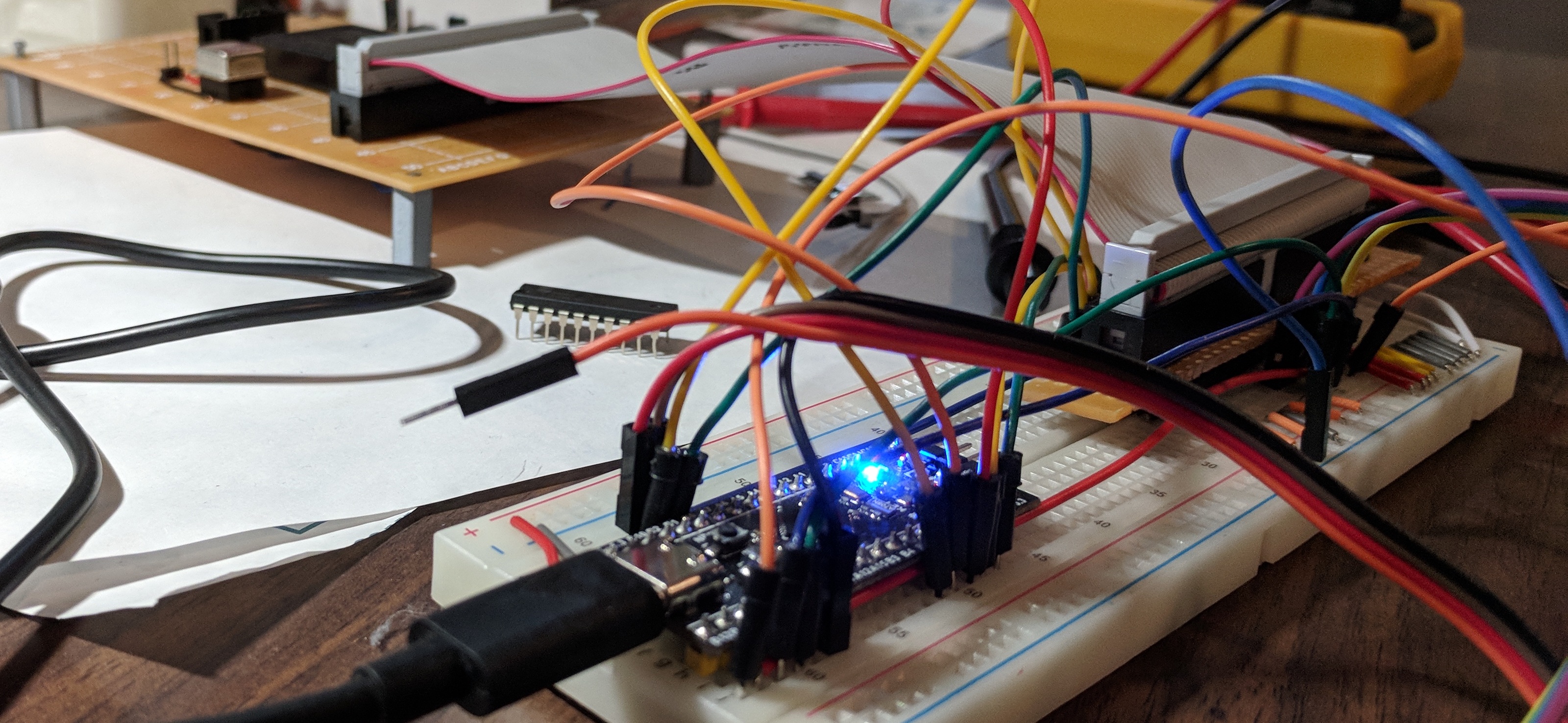
To flash the device, I’m programming over USB. I could use the SWDIO pins for this, which would give me debugging support too. However, those pins don’t supply power, and I’d need to run the USB cable anyway. The open-source [dfu-util][dfu] tool will program many ST devices, including the STM32F4 using the bootloader. The STM32F4 can be reset to boot from the bootloader by asserting BOOT0 during a reset (with BOOT1 low). The Black Pill board has a button for this purpose, and pulls BOOT1 (aka PB2) low at all times. Programming the board via USB is as simple as holding BOOT and pressing NRST, then using a magic invocation of dfu-util to flash my binary image at the right address, into the right device target.
Experiments
Because I have no facility to test register configuration, I’m taking a cautious approach. I’ve commented out all code to write to the clock configuration registers, leaving only the timer output. With the HSI running at 16MHz, I expect to see a signal of .

I made several mistakes, which isn’t entirely unexpected. I can’t debug on the device itself, because my st-link clone appears to be broken, possibly fried by my own actions, but I can inspect my code in a debugger.
The first problem is that my linker script wasn’t quite right. You are free to name your output sections anything you like, and I chose .vectors for my vector table. However, that freedom is limited by your output format. In an ELF binary, however, certain section names are magical.
Idx Name          Size      VMA       LMA       File off  Algn
  0 .vectors      0000001c  08000000  08000000  0001803c  2**0
                  CONTENTS, READONLY
  1 .text         000000dc  08000000  08000000  00010000  2**2
                  CONTENTS, ALLOC, LOAD, READONLY, CODE
  2 .rodata       00007f60  080000dc  080000dc  000100dc  2**0
                  CONTENTS, ALLOC, LOAD, READONLY, DATA
  3 .ARM.attributes 00000021  00000000  00000000  00018058  2**0
                  CONTENTS, READONLY
As I planned it, my .vectors section is at VMA 0x08000000, hooray. But its flags don’t include ALLOC or LOAD, so the section is never loaded into memory, or flashed onto the device. Instead, the .text section is loaded at VMA 0x08000000, and the processor attempts to jump to 0x60b00000 to run code, as shown in gdb with x/2xw 0x08000000. This does not succeed. The problem is easily solved: I put the .vectors input section into the .text output section.
The next problem is in this little excerpt of code, that is supposed to set pin A2’s mode to its alternate function.
        ldr     r0, [r6, GPIOx_MODER]
        orr     r0, r0, GPIOx_MODER_MODE_ALT
        str     r0, [r6, GPIOx_MODER]   // set PA2 to mode AF
Symbolic constants abound. I can check those by cross-referencing where they’re defined, but I can also fire up a debugger and look at what code is in the byte stream.
0x080000a2 <+46>:	ldr	r0, [r6, #0]
0x080000a4 <+48>:	orr.w	r0, r0, #2
0x080000a8 <+52>:	str	r0, [r6, #0]
#0 is the right offset for GPIOx_MODER, but what’s this? #2 is definitely not the right constant for setting pin 2 to AF - it’s the right constant for setting pin 0 to AF. I neglected to shift my symbolic constant into the right spot for the pin I want to affect.
orr r0, r0, GPIOx_MODER_MODE_ALT << 4And now, I see output.

I see the output I predicted, no less. The time there is 2.625μs, which is exactly 42 divided by 16. Every few intervals, the measured frequency is 375KHz, which I would expect is because either the internal oscillator or my cheap logic analyser’s clock are not perfectly accurate. A 2.625μs measurement is 63 samples at 24MHz, while a 2.667μs measurement is 64 samples.
Changing clocks
Able to see output, it’s now time to start changing my clock speeds. I’ll start by verifying I can change the APB1 divider, because that’s the one I need to get right before mucking with the system clock. This means re-including stores to RCC_CFGR. While I’m there, I’ll also turn on the HSE and wait for it to be ready, and as the last thing I do in my main, I’ll turn on PC13 as a push-pull output, driven low, to turn on the board’s blue LED. This will give me a quick visual indicator that my code has made it through all of the configuration, instead of hitting a trap or an endless loop.
With the APB1 divider set to 2, I now expect to see 5.25μs between peaks, a 190KHz rate, taking 126 samples. I may see 189KHz as well, which is 127 samples. Let’s take a look.
Well, hmm. Am I failing to configure the APB1 clock divider? If so, how? A peek at my code shows I forgot to actually set r6 to RCC, so I’m attempting to set the clock by writing a word into Flash. This does not succeed. I fix that up, and…
Uh. Well, it’s midnight, I should sleep.
Finding the mistake
There is a very good reason for the timer output being unchanged despite the APB1 clock divider being set to two. The reason for it is right there on the clock tree diagram from the last post: the timers on APB1 and APB2 have their clocks multiplied by a value that’s set by the microcontroller, based on the APBx prescaler. From the reference manual (RM0368 rev. 5, p94):
If the APB prescaler is configured to a division factor of 1, the timer clock frequencies (TIMxCLK) are set to HCLK. Otherwise, the timer clock frequencies are twice the frequency of the APB domain to which the timers are connected: TIMxCLK = 2xPCLKx.
So it turns out that I am seeing what I would expect to see if I set the APB1 divider to 2.
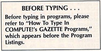
It’s also around this point that I reflect on the fact that my logic analyser has eight inputs, and I’m only using one. I can observe both TIM9 and TIM2 at once. I’ll use PA3 for TIM9 channel 2, and switch to PA1 for TIM2 channel 2, so I can re-use the timer setup code trivially.
With a big change to my port setup code, I’ll check my constants via gdb again:
   0x08000088 <+32>:	ldr	r6, [pc, #108]	; (0x80000f8)
   0x0800008a <+34>:	mov.w	r0, #204	; 0xcc
   0x0800008e <+38>:	str	r0, [r6, #8]
   0x08000090 <+40>:	movw	r0, #12304	; 0x3010
   0x08000094 <+44>:	str	r0, [r6, #32]
   0x08000096 <+46>:	ldr	r0, [r6, #0]
   0x08000098 <+48>:	orr.w	r0, r0, #136	; 0x88
   0x0800009c <+52>:	str	r0, [r6, #0]
Address 0x80000f8 has the right value for GPIOA. 0xcc is 1100 1100, which sets very high speed on pins 1 and 3. 0x3010 is 0011 0000 0001 0000, written to GPIOx_AFLR, sets pin 3 to AF03, and pin 1 to AF01. And finally, 0x88 is 1000 1000, written to GPIOx_MODER. This assumes the modes for pins 1 and 3 are in their reset state, and sets them to AF mode.
With APB1’s clock now divided by four, I’m ready to run this sucker.
I configured both timers with prescale 7, counter 6. With APB2’s timers running twice as fast as APB1’s, I now expect to see TIM9 spitting out a 381KHz signal, and TIM2 spitting out a 190KHz signal.
The rest of the owl
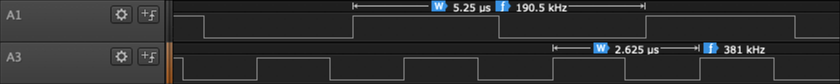
With the most risky part out of the way, it’s time to fire up the whole configuration scheme and get the part running at 84MHz. I’ve set APB2’s divider back down to two, which means both TIM2 and TIM9 will be running at 84MHz. The settings I have for prescaler and counter should produce a 2MHz signal (84/6/7 = 2).
Now I need to refer back to my notes so I can start reacting to signals. The pins I’ve defined are:
| STM32 | Z180 | Purpose |
|---|---|---|
| PA0:7 | D0:7 | Data bus, in/out |
| PA9 | - | STM32’s “processing read” flag |
| PB0:1 | A0:1 | First two address lines |
| PB5:10 | A2:7 | Next six address lines |
| PB12 | IORQ | |
| PB13 | MREQ | |
| PB14 | WR | |
| PB15 | RD |
Note: the mistake I made in the previous post to somehow forget that the address bus is 16-bits continues here. I won’t fix it, I’ll live with it and move on to using real memory.
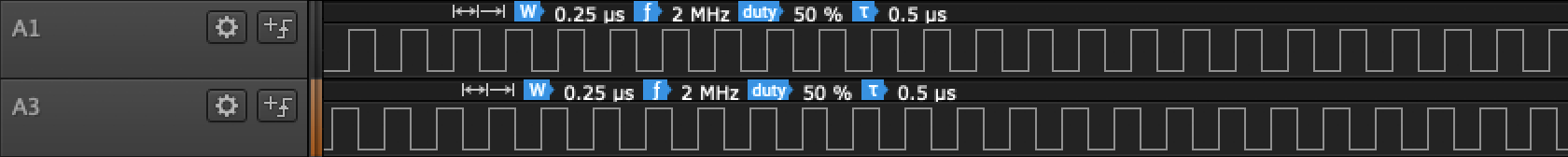
The code to watch for a memory request and react to it is straightforward. I read from the GPIOB input data register and check to see if MREQ and RD (bits 13 and 15) are set. If not, I loop and read again.
If so, then I set PA9 using the bit set/reset register for GPIOA, then I wait for either MREQ or RD to clear. I then reset PA9, and loop back to wait for MREQ and RD again.
loop:   // wait for MREQ and RD to be set
        ldr             r0, [r6, GPIOx_IDR]
        ands            r1, r0, 0b1010000000000000
        beq             loop

        // set PA9 to indicate memory read is active
        ldr             r0, =1 << 9
        str             r0, [r5, GPIOx_BSRR]

reading:// wait for MREQ and RD to go inactive
        ldr             r0, [r6, GPIOx_IDR]
        ands            r1, r0, 0b1010000000000000
        bne             reading

        // reset PA9
        ldr             r0, =1 << 25
        str             r0, [r5, GPIOx_BSRR]

        b               loop
There’s a logic error in here I introduced in the 11th hour, so it works almost as expected. The logic analyser’s capture shows the STM32 dropping PA9 low when MREQ and RD are low, and PA9 staying high during a DRAM refresh cycle when only MREQ goes low. Of course, I wrote it thinking I was asserting PA9 high when MREQ/RD were active, but I forgot to take into account that these two lines are active low. Despite this, the timing here shows the STM32F4 will comfortably respond to a read request in time, and have no trouble turning output off when it should relinquish the bus.
A few other things have gone a little bit wrong, of course. I was having trouble getting the STM32 to boot up correctly: it would only work immediately after being flashed on. Turns out I forgot to uncomment the Flash wait state register write, which as promised crashes the μC. I have to plug in the STM32’s USB cable before the logic analyser: I suspect a ground loop is at fault. And my ghetto breadboard header for the 50-pin IDC socket is really not a good piece of engineering, so A1 isn’t wired up right. This final point means I’ve got to bust out a soldering iron before I can make the STM32 act as RAM and ROM.
I also don’t really like my chances of fitting enough wires on this breadboard to wire up the data lines via a ’245. Another round of fiddly soldering of 40 or so wires, here I come.
This experiment has been a great success. I’ve programmed my STM32F4 from the ground up, detected the Z180’s memory requests, and confirmed that an 84MHz μC is easily fast enough to be RAM and ROM for a 1MHz processor. Nice.
| Budget | CPU | Power | Keyboard | Video | Memory | Debug |
|---|---|---|---|---|---|---|
| $209.35 of $400 | ██── | ──── | ──── | ──── | ──── | ███─ |