
The TRS-20 - Timing check
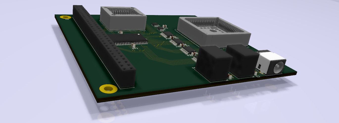

I am working on the CPU board design, which covers too many topics and decisions to fit into just one post. This particular post explores timing in depth, checking that I understand how fast my logic circuits must be to keep the bus contention free and the CPU state valid.
But first, a digression…
When, say, an adder circuit in a CPU is presented with some values on its input wires, some brief amount of time will elapse before the correct value presents on its output wires. In the meantime, it’s even possible that the output value will pass through intermediate states before settling on the right answer. The clock in a processor is the solution to this: it doesn’t matter what the circuit does while computing its answer, so long as it’s got the right answer by the time the next clock transition happens. The clock signal synchronises all the circuits of the processor, shuffling data from circuit to circuit with metronomic regularity.
When you pop out of the CPU and look at its immediate peripherals, the clock signal comes along for the ride. External components must march to the same drum as the processor, consuming data it outputs before the processor has moved on to the next task, and providing data as input before the processor acts on it.
This manifests in data sheets and other documentation as timing diagrams. These diagrams have time as the horizontal axis, and signal levels as the vertical axis, with multiple signals on the same diagram to show how the signals must synchronise with each other. If there’s a clock synchronising the signals, it’ll usually be the first signal in the diagram. Since the diagram’s purpose is to show relative timing constraints, the time axis isn’t accurate - if two signals change at the same point horizontally, they’re only specified to change at the same time if the diagram indicates a zero time delay between them.

A timing diagram’s value is in explaining how one signal’s change in state is related to another signal. In the above diagram, a table would give an upper or lower bound for the intervals marked 1 and 2. An upper bound for interval 1 would specify the maximum time that the address lines will settle after the rising edge of T1. A lower bound for interval 2 would specify the minimum time that the address lines will be settled before /MREQ falls.
Processor timing details for the Z180
For the Z180 processor, there’s a feast of timing diagrams to dine on. They get their own section of the User Manual, and are one of the few pieces of information that appear in both the User Manual and the specification document. They’re accompanied by large data tables specifying bounds for various durations in the diagram. Time value tCYC is the clock cycle time - the time between each rising edge. For the Z8L180-20 tCYC lies between 50ns and DC, reflecting that the maximum speed of the processor is 20MHz (), and there is no minimum speed: you can stop its clock entirely.
Some of these timing values tell me useful information for my board design - my clock should be able to satisfy not only the clock cycle time bounds, but also the high and low pulse width bounds, which are only specified as minimum values. The Z80180 expects that the low and high pulses are each at least 40ns long. The upper bound is determined by the actual clock cycle time and the other pulse time minimum - for a 100ns cycle, the maximum high or low pulse is 60ns. There’s also clock rise and fall times: signal levels don’t change instantaneously, and if they transition too slowly a CMOS input can oscillate between reading a high and a low, or if you’re lucky, just chew up relatively huge amounts of power.
Others of these timing values tell me useful information for my component selection, when read in conjunction with a timing diagram. How fast does my SRAM have to be if I want to access it with no wait states? Well - in an opcode fetch cycle, the address pins will stabilise no more than tAD (30ns) after the first rising edge of the first clock cycle of the opcode fetch machine cycle, and no less than tAS (5ns) before /MREQ or /IORQ falls. In turn, /MREQ promises it will fall no later than tMED1 (25ns) after the falling edge of that first clock cycle. Similarly, tRDD1 (25ns) promises that /RD will fall at most that long after the falling edge as well. There’s nothing tying /RD and /MREQ together though, so there’s no commitment made as to which will fall first, or how much time will elapse between the two falling.
It’s all a bit complicated. Perhaps a diagram would help…
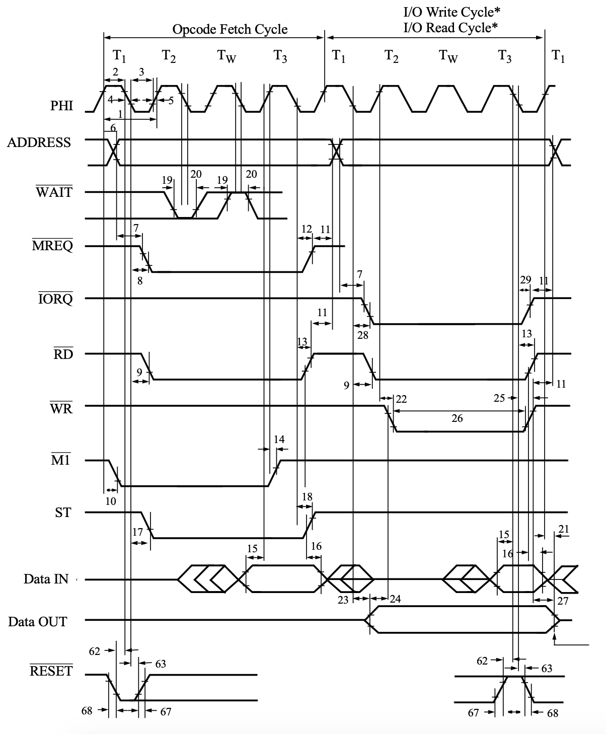
There’s a lot going on in this one diagram, but I can use it to produce the information I really need - if I have 12ns SRAM, how fast does my glue logic have to be before I need a wait state? And for my Flash ROM and any on-board I/O devices, similar questions play out.
Working out maximum delays
The figure I included above shows an opcode fetch cycle and I/O read/write cycles, but not a memory read or write cycle. As it turns out memory read cycles look almost the same as opcode fetch cycles with one key difference - the data lines are sampled on the falling edge of T3, not the rising edge. Taking a leaf from Application Note AN009602-0808 (“The Z180 Interfaced with the SCC at 10 MHz”) a simplified diagram showing a read and a write memory cycle will clear up the clutter nicely and show just what’s needed for memory timing constraints.
| No. | Label | Time | Purpose |
|---|---|---|---|
| 6 | tAD | ≤ 30 | PHI rise to Address Valid Delay |
| 7 | tAS | ≥ 5 | Address Valid to /MREQ or /IORQ fall |
| 8 | tMED1 | ≤ 25 | PHI fall to /MREQ fall delay |
| 9 | tRDD1 | ≤ 25 | PHI fall to /RD fall delay |
| 11 | tAH | ≥ 5 | Address Hold time from /MREQ, /IORQ, /RD, /WR high |
| 12 | tMED2 | ≤ 25 | PHI fall to /MREQ rise delay |
| 13 | tRDD2 | ≤ 25 | PHI fall to /RD rise delay |
| 15 | tDRS | ≥ 10 | Data Read Set-up time |
| 16 | tDRH | ≥ 0 | Data Read Hold time |
| 22 | tWRD1 | ≤ 25 | PHI rise to /WR fall delay |
| 23 | tWDD | ≤ 25 | PHI fall to Write Data Delay time |
| 24 | tWDS | ≥ 10 | Write Data Set-up time to /WR fall |
| 25 | tWRD2 | ≤ 25 | PHI fall to /WR rise delay |
| 27 | tWDH | ≥ 10 | Write Data Hold time from /WR rise |

The only timing not specified in the table above is 1 (tCYC, the clock cycle time). I will use an 18.432MHz MEMS oscillator, the DSC1001DE5. This part is accurate to 10ppm, which means tCYC will fall between 54.253ns and 54.254ns, which I will call 54ns. It outputs 0.9xVDD, or 2.97V, with a rise and fall time no longer than 2ns. The duty cycle could be anywhere between 45% and 55%, or 24.3ns to 29.7ns.
A regular memory read cycle shortes the data window by only requiring that data has been set up tDRS before the falling edge of T3, rather than the rising edge. I/O read cycles are the same as regular memory read cycles, except that /IORQ replaces /MREQ and there is always at least one wait state. In Z80-compatible mode though, /IORQ and /RD fall after the rising edge of T2, so that’s a little trap to be wary of.
To read a byte from a typical memory chip, one will decode the address lines plus /MREQ to activate the chip enable input of the memory, then activate either output enable or write enable depending on whether /RD or /WR is active. /MREQ activates 5ns after the address lines have settled, or 25ns after T1 falls. T1 could fall as late as 29.7ns after T1 rises, so /MREQ will not become active until 54.7ns have elapsed. /RD will become active at the same time. This is 1.7ns after T2 has begun, leaving 53.3ns until T3 begins, and 43.3ns until the data must be available.

This 43.3ns is eaten up by address decoding to drive the SRAM’s /CE input, by any logic required to translate the CPU’s /RD and /WR outputs into the SRAM’s /OE and /WE inputs, by any buffering or logic level conversions required, and of course by the SRAM’s own timing constraints. Fortunately, these are easier to understand - in a nutshell, data will be ready at most 10ns after /CE is active and 6ns after /OE is active. The data outputs will be Hi-Z again 5ns after /OE goes high. These figures are specific to the SRAM chip I’m using: check your datasheet.
There’s also parasitics that add delay to the signal. On my sized board, this will be well below 3.3ns - the speed of signals on stripline traces is close to 150mm/ns, so it’ll take less than one nanosecond for a signal to traverse my 10cm^2 board corner to corner. This leaves me a tidy 40ns to work with.
For SRAM, this is an enormous surplus of time, with a whopping 30ns available for logic. For Flash ROM, it’s not so much time. My chosen ROM is the SST39SF020A, a 2Mbit 55ns IC. 55ns is, of course, greater than 40ns. But all is not lost, because as with the SRAM the 55ns applies from the time /CE is active. Data will be available 35ns after /OE is active, so if I can decode the address lines and toggle /CE early enough I will have 5ns to activate /OE on the ROM and still have data available inside the zero wait state window. Data must be ready at t+98ns and the address lines are settled at t+30ns, leaving 10ns for address decoding and 3ns for parasitics.
The Z180 has a 16-bit I/O space so A16-A19 should all be low for any I/O request. Address decoding on ADDR alone can be fairly sure that if the ROM bits are set (A18, A19) that it’s really going to be a ROM request. In a similar vein, if A18 is set and A19 is clear it’s going to be an off-board memory request, and a wait state could be immediately generated, but I’m quite comfortable requiring software to manage this via the CPU’s wait state generator if off-board memory is needed.

When writing, the SRAM IC has from the fall of /WR to the fall of T3 to store data. /WR should fall no later than t+79ns, and T3 should fall no earlier than t+131.4ns. /WR will rise up to 25ns later. Timing constraint 26 (tWRP, write pulse width) guarantees that /WR will be low for at least 80ns. You could almost write the byte down on paper with that much time.
Wait state generation
Wait states are inserted between T2 and T3, either because the Z180’s internal wait state generator has been configure to insert them, or because the /WAIT signal is low when sampled at the fall of T2. The internal wait state generator can add zero to three wait states to every memory or I/O access, with three being added at reset.
The /WAIT signal must be asserted low at least tWS (15ns) before T2 falls, and held low at least tWH (10ns) after T2 falls. To allow the processor to continue, it must be de-asserted at least tWS before a TW clock cycle falls, and held high at least tWH after it falls.
T2 could fall as early as t+78.3ns, and /WAIT must be asserted low 15ns before that at t+63.3ns. If /WAIT is asserted in response to /MREQ falling at t+54.7ns then only 8.6ns is available. /WAIT transitions are ideally done on the rising edge of a system clock, but /MREQ might fall after T2 rises - if wait states are required for a memory read, they are likely to need to be generated either based on address alone or done using the internal wait state generator. For IO, there’s already one wait state inserted at a minimum, giving at least 62.6ns.
Interrupt acknowledgement
The Mode 0 and Mode 2 INT0 acknowledgement cycles both read a data byte from the bus, where only M1 and IORQ go low. In both cases there are two wait states, /M1 falls up to 35ns after T1 rises, /IORQ falls at least 125ns (2.5 clock cycles) after /M1 falls and at most 25ns after TW1 falls. Data must be ready 10ns before T3 begins to rise. Assuming TW1 falls late at 29.7ns and /IORQ falls 25ns after that, and a few ns for parasitics, there’ll be 40ns left in which to respond to the acknowledgement cycle with data on the bus.
Memory writes
- 10 tM1D1 PHI rise to M1 fall ≤ 35ns
- 28 tIOD1 PHI rise/fall to IORQ fall ≤ 25ns
- 29 tIOD2 PHI fall to IORQ rise ≤ 25ns
- 30 tIOD3 M1 fall to IORQ fall ≥ 125ns
IO timing
IO read and write cycles differ from memory only by the addition of one mandatory wait cycle. This adds 54ns to all timing constraints. In the case of tWRP, the minimum write pulse time is 150ns.
Timing constraint summary
| Constraint | Description | Time |
|---|---|---|
| Mem read | ADDR to data available | 65ns |
| Mem read | /MREQ, /RD fall to data available | 40ns |
| Mem write | /WR fall duration | 80ns |
| Mem wait | /MREQ fall to clock rise | -0.7ns |
| IO read | /IORQ, /RD fall to data available | 94ns |
| IO write | /WR fall duration | 150ns |
| IO wait | /IORQ fall to clock rise | 50ns |
| INT0 read | /M1 and /IORQ fall to data available | 40ns |