The TRS-20 - Assembling the board

I have all my parts, I have my boards, it’s time to assemble this thing. I’ll be starting with the highest risk components first, on the grounds that if I muck up I will have less to replace to try again.
Soldering, round one
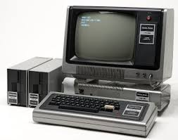
I’ve attempted the iCE40 IC first, as the most likely to fail. And indeed, it hasn’t gone at all well. There were terrible solder bridges on two sides, and while I’ve eventually figured out the technique for dealing with these I’ve applied substantial heat to get there. The board looks in good nick, perhaps due to the two large inner copper planes wicking heat away, but there’s a persistent short from 3.3V to GND that, obviously, is a deal-breaker. I’ve tested the other four boards and they’re all short-free so it’s very likely this is a soldering issue. I found and removed another short on two address lines, and think everything else is clear (no test points - a board design issue), but I don’t even know which of the supply/ground pin pairs has the short. I fear it may have somehow happened beneath the IC where I can’t see it, or with excess heat down a ground via delaminating the board enough for solder to worm its way to a connection with the power layer. It may just be solder sitting sneakily behind some pins, but there’s only two supply pins that are adjacent and I’ve inspected the everloving out of them both.
I’ve ordered three more FPGAs, and I’ll try again, armed perhaps with a greater fear of excessive solder paste, a new multimeter that doesn’t have one lead replaced by an alligator clip holding a screw, and my improved techniques for fixing small bridges. They won’t arrive until the end of the week, so I’ve put board assembly aside for now.
Programming ROMs
I have two ROMs to program: the bitstream to configure the FPGA (assuming I ever get it soldered on safely) and the boot/BIOS ROM. The bitstream ROM is programmed over SPI, and is a DIP-8 in a socket. I’m fairly confident I can solder up something to program bitstreams using my STM32F401 black pill board. The boot/BIOS ROM is a bit more difficult, as it’s a parallel device with 18 address pins, 8 data pins, and a little assortment of control pins. I’ll need shift registers to handle this. Luckily I have a little pile of 74HC595s lying around unused. Two of those gives me 16 of my 18 address pins at the cost of two µC pins, and two more for A16 and A17. I can wire up the µC directly to the data pins, and to /OE and /WR, and I’ve only used 14 pins.
I will load up a perfboard with sockets, and then have to figure out how to have the STM32 read a programming bytestream over USB serial. But this can wait while I perform main board assembly - I don’t need more parts, just more time.
I’m also slowly working on a TRS-20 emulator, so I can crack on with writing a boot ROM that’s got a halfway decent chance of actually running on the real deal.
Soldering, round two
My replacement FPGAs arrived earlier than expected. I got in plenty of practice on the first board for dealing with 0.5mm pitch pins using an iron and absurd amounts of flux, so I thought I’d try drag soldering one. Now I have two badly soldered FPGAs on two boards. I don’t really think it’s worth trying to fix the second IC it’s that bad, and the first has been subject to so much heating and cooling and still has a sneakily hidden bridge somewhere between 3V3 and GND.
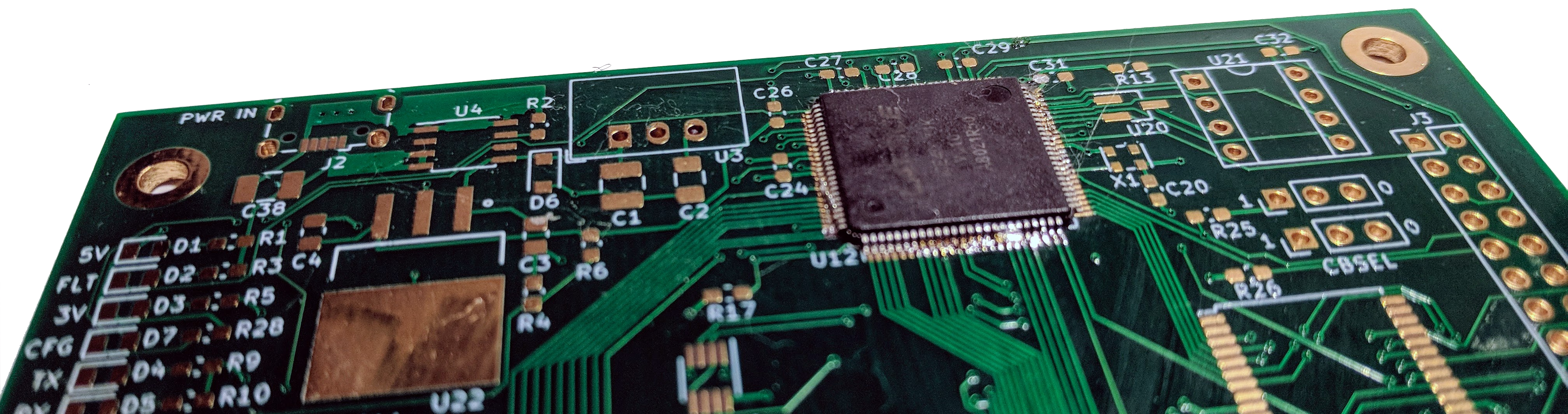
I tried a third FPGA on a fresh board. I have one spare FPGA and two spare boards. This time, I carefully lined up the IC then used a toothpick to put as little solder paste on as I could, then cracked in with the heat gun. There were a few bridges left, but this time I was able to get in and clean them up without using crazy heating cycles. I’ve checked all 100 pins to confirm they’re connected to what they should be, and not to what they shouldn’t be, and it’s all looking good.
So I got stuck into getting a few more components on the board. I have absolutely no idea if my 100MHz oscillator is on right. It’s a tiny QFN - the only no-lead part on the board - and I can see that at least two pads are soldered, the others probably are, and maybe it doesn’t have bridges, or heat damage from the hot air gun. I can’t really test it, and I didn’t have any particular use for it.
The 1.2V regulator is a DDPAK, an absolutely enormous beast of a part. It features a large tab for heat transfer, and again I can’t see underneath it to know if solder paste melted or not. The DDPAK is designed to dissipate heat, so it fights every step of the way when soldering. Even the three pins wick heat magically away into the large copper pours and are difficult to solder. It’s on - but the tab might not be soldered down as well as it should be.
I am filled with regrets about choosing to use 0603 bypass capacitors, they’re fiddly. I’ve put on a half dozen or so, plus a few larger capacitors around the power management. My goal is to get enough soldered on to verify the power circuitry, and then to verify the FPGA is on safely, so I’ve done the DDPAK, the eFuse, and capacitors. I’ve yet to do the resistors, diode, and the R-78 3.3V regulator, more caps, and perhaps the MIC803.
That’s all for another day.
Soldering, round three
It is another day. I’ve pressed on, popping on a stack of resistors for the LEDs, eventual I2C bus pull-ups, CDONE pull-up, and power management resistors. I’ve finished off all the capacitors for the regulators, the FPGA, and its ROM. I’ve added the ROM’s socket, and an unprogrammed ROM is sitting in it, tempting fate. I’ve also added the power USB port, which in hindsight I should have done before the whopping great big capacitor that made access to the USB pins much harder than I’d have liked. All of it went pretty well, I only lost one 0603 resistor (and found it again when cleaning up, amazingly), most of my parts aren’t on too crooked, and there’s no shorts or, as far as I can determine, bad joints.
And finally, I added one LED, the power indicator LED. This is my first SMD LED, and finding the polarity of these parts proved a little harder than I’d expected. The data sheet said the underside would indicate the cathode with a single horizontal line, but the actual underside had a turnstile symbol instead. I wound up relying on the advice in the sheet that the anode is closest to the holes on the tape.
It is time to apply power. If I’ve done anything wrong in design or assembly, magic smoke will now escape.
Powering up, round one
I pushed the USB cable into the socket, fearing the worst, hoping for the best. Today, I got the best: the power LED lit up. The board has juice! This LED is wired straight to the USB power supply, so it tells me that I don’t have a critical short somewhere, and that I do have a successfully soldered USB port, resistor, and correctly oriented LED. That’s quite a moment, but not the end of the story, not just yet.
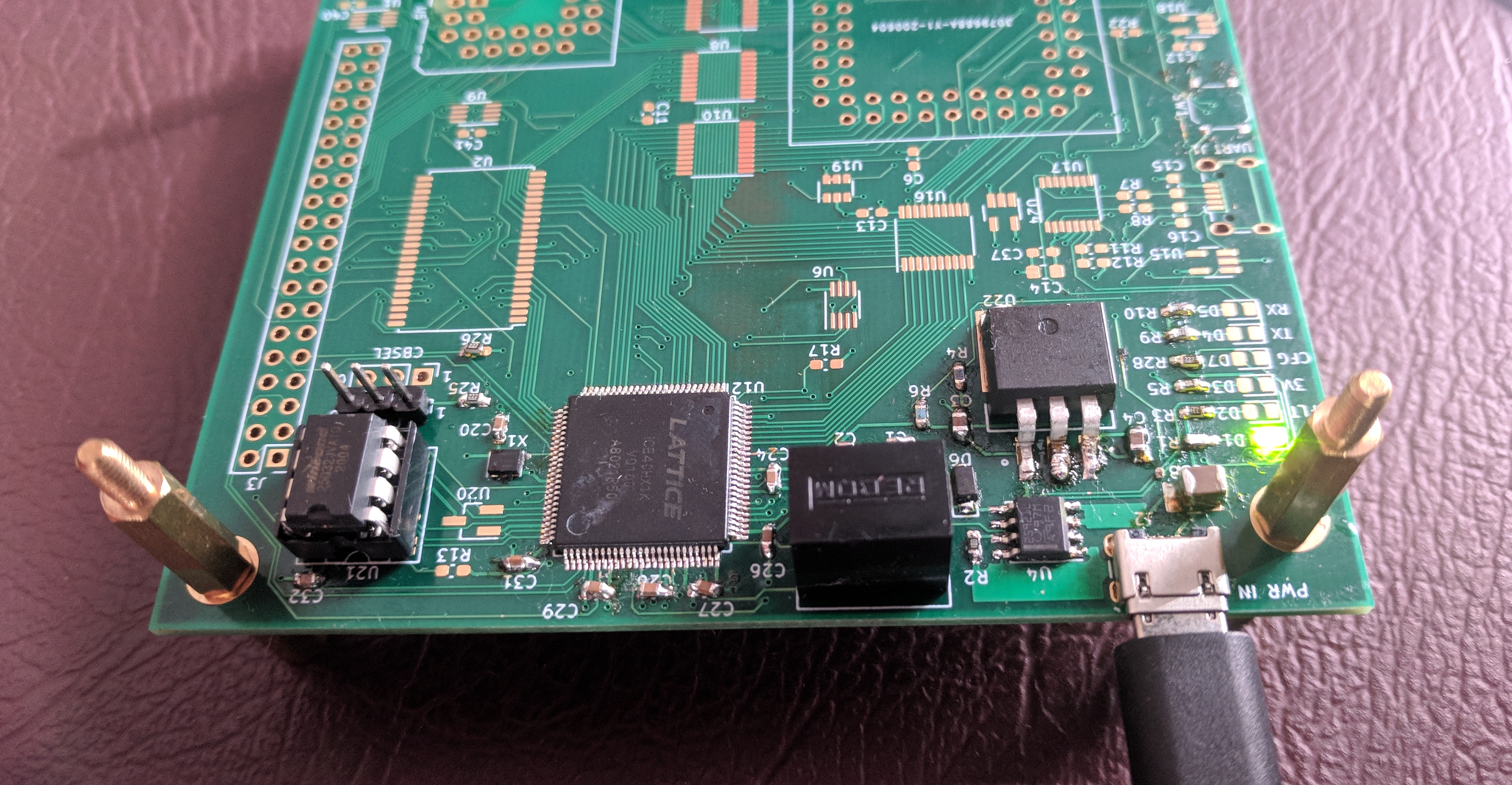
I have two regulators and a voltage divider network in my power circuitry. The RECOM should be converting the 5V supply from USB via the eFuse into 3.3V, while the DDPAK linear regulator supplies 1.2V from the same source. I gave them both a probe with the multimeter, and to my delight, both are showing the expected levels. The voltage divider for the MIC2774 reset controller is also performing properly, delivering 315mV to the 300mV comparator input. Nothing is unduly warm, so I feel confident in declaring my power circuitry design and assembly a success.
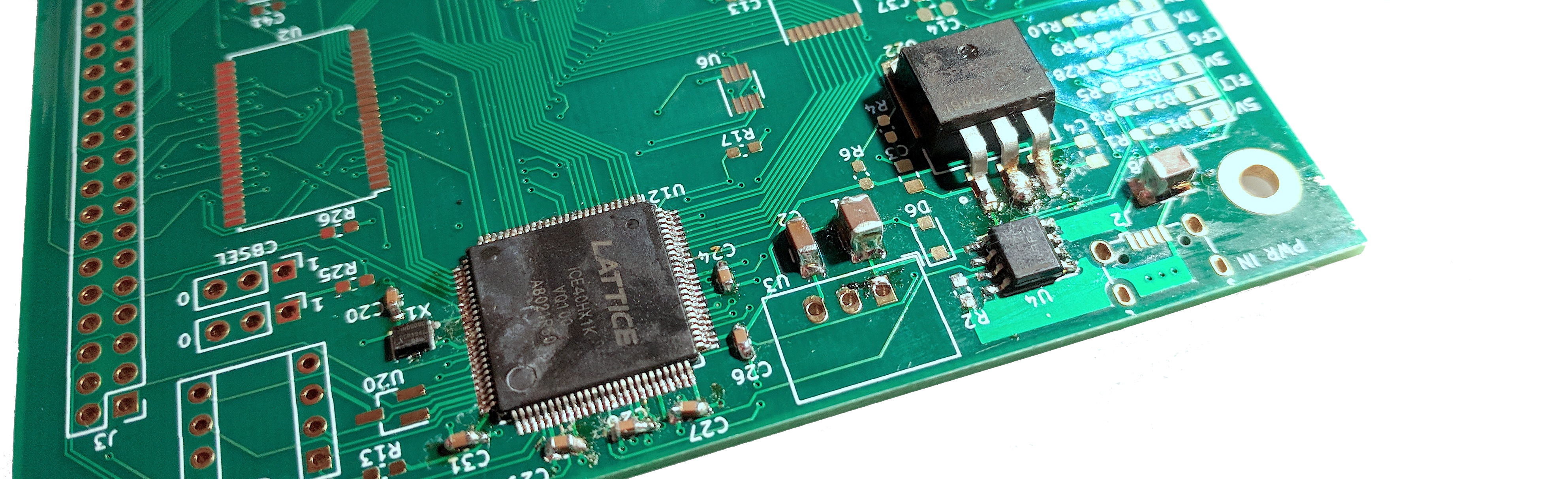
I have no idea just yet whether the FPGA, ROM, and 100MHz oscillator are in a good place. Tomorrow’s soldering task will be to add the remaining LEDs (including the two USR LEDs wired to the FPGA), the MIC803 supervisor, and the pull-up for the ROM’s Slave Select that I missed - U20 and R13 in the above image. After that I’ll choose between testing the FPGA out before committing RAM, ROM, and CPU, or pressing on with the actual computer part of this circuit.
The ROM programmers are becoming more important with every additional blob of solder hitting the board.
Soldering, round four
This time I’m methodically placing capacitors and resistors, aiming to complete all of each particular size. I’ve knocked out the 0.1µFs, although one is dangerously close to forming a bridge and needs fixing. I’ve put on all the 10kΩ and 2.2kΩ resistors - including deciding that I would use 10kΩ for the /INTx pull-ups instead of 2.2kΩ. I’ve finished all the LEDs off, five are the yellow-green diffuse diodes and three are green low-current clear. The clear LEDs have a dome on top which makes them a little fiddly to hold in place for hand soldering, but didn’t give too much trouble. I also put in the MIC803, which I realised I’d made harder for myself by soldering the SPI Flash socket in place first. There wasn’t much room to get in and heat it up, and it took a few goes to ensure the pin near the socket was adequately wetted.
I put on the 10kΩ resistor R12, which forms part of the voltage divider for VBUS sense on the FT230X USB chip. Since the FT230X isn’t currently programmed for VBUS sense, this means I’ve wired up an output chip with a resistor into GND, and this will draw 0.33mA current when that output is HIGH. I need to be careful not to solder on R11 until I’ve programmed the IC.
Foolishly, I also soldered on the PLCC-32 socket. Progress is barely visible after doing a few tens of 0603 parts, so I wanted some big visible progress in place. However, this is now going to get in the way for soldering the ICs close to the socket: U1 and U30 are SOIC8 ICs with one side of pins each about 7mm away from the socket. They’re handsolder pads, at least, so it should be okay, but I need to take the lesson to heart and not rush in to the big parts until I’ve dealt with the parts needing easier access.
Sadly, on power-up my LEDs didn’t light up as expected. 5V is still lighted, which is good news, but 3V didn’t light up while both USR LEDs wired to the FPGA did, albeit not as bright as the others. Since my understanding of the FPGA is that every IO pin goes Hi-Z during configuration, this seems like terrible news - if power is coming through that IC might be on the fritz. I re-read the iCE40 Programming and Configuration Guide, which does definitely say those pins are Hi-Z with pull-ups. The iCE40 family data sheet says both that I/O pins default to weak pull-down and weak pull-up, depending on which part of the sheet you’re at, but clearly these two pins at least are not wired to GND. There are 2.2kΩ resistors on those LEDs already, so for them to be visibly lit up the weak pull-up resistors can’t be that weak - or the FPGA might still be on the fritz.
The 3V LED was nothing more serious than a bad solder joint on one side, easily fixed.
At this point I’m confident that everything on the board so far has been soldered on correctly (if not necessarily neatly) but I have some doubts about whether the FPGA is still good, or if it’s been fried by clumsy handling or soldering. My next work is therefore going to focus on programming the SPI Flash ROM with a bitstream that can demonstrate the FPGA is good.
Errata
- U7 has four floating pins that will become inputs if /BUSACK is active, and four pins that will be outputs wired directly into ground. I can perhaps fix it by also wiring the floating pins to ground - without doing that, using /BUSRQ might result in a short through the ’245 buffer.
- There’s no solder mask between the pins of most of my SMD ICs. It’s not a critical failure by itself, but it significantly increases the risk of solder bridges. This may have contributed to my difficulty with the iCE40, and may cause problems for the 0.65mm pitch ICs I have yet to do.
- The reset button. I didn’t check pins on this part, and they’re wrong. When the button is soldered on the reset input on the supervisor is always pulled low. I may try to jury rig something down the line, but for now I will just go without.
Potential improvements
- Yanking a USB cable in and out for power is not great. I considered a power toggle switch, but chose to omit it - I think putting one in would be a substantial improvement.
- The FPGA’s default pin state includes pull-ups; the USR LEDs are on at boot, until configuration is complete. Inverting these LEDs to be wired to +3.3V with an open drain pin configuration would prevent this.
- The CBSEL jumpers could have been spaced 2.54mm apart and used a double row pin header, or perhaps DIP switches, though I wanted something with low chance of mechanical failure.
- There’s a row of resistors for pull-ups that could have been replaced by two resistor arrays to take a bit less board real-estate up. Fixing U7’s floating and shorted pins will require resistor arrays to fit without major board layout changes.
- The 100MHz oscillator in a QFN package is difficult, as I expected it would be. It’s also more important than I counted on, as it’s the only available clock for the FPGA without the processor’s PHI output. Using a bigger package for this oscillator would be a good change.
Budget summary
The budget is blown. I bought three more iCE40HX1Ks to cope with my first failure at soldering, I forgot I needed PLCC-32 sockets, and for the ROM programmer I’ve also had to buy replacements for failed parts. I’ll track my total spend and when I’ve either succeeded or admitted defeat on the CPU board I’ll tally the cost in parts for just the board, but I will no longer pretend I’m going to build a retrocomputer for $400.
| CPU | Power | Keyboard | Video | Memory | Debug |
|---|---|---|---|---|---|
| ███─ | done | ──── | ──── | ███─ | done |