The TRS-20 - Finishing assembly

I claimed in the last post that, with blinking lights achieved, the job was done.
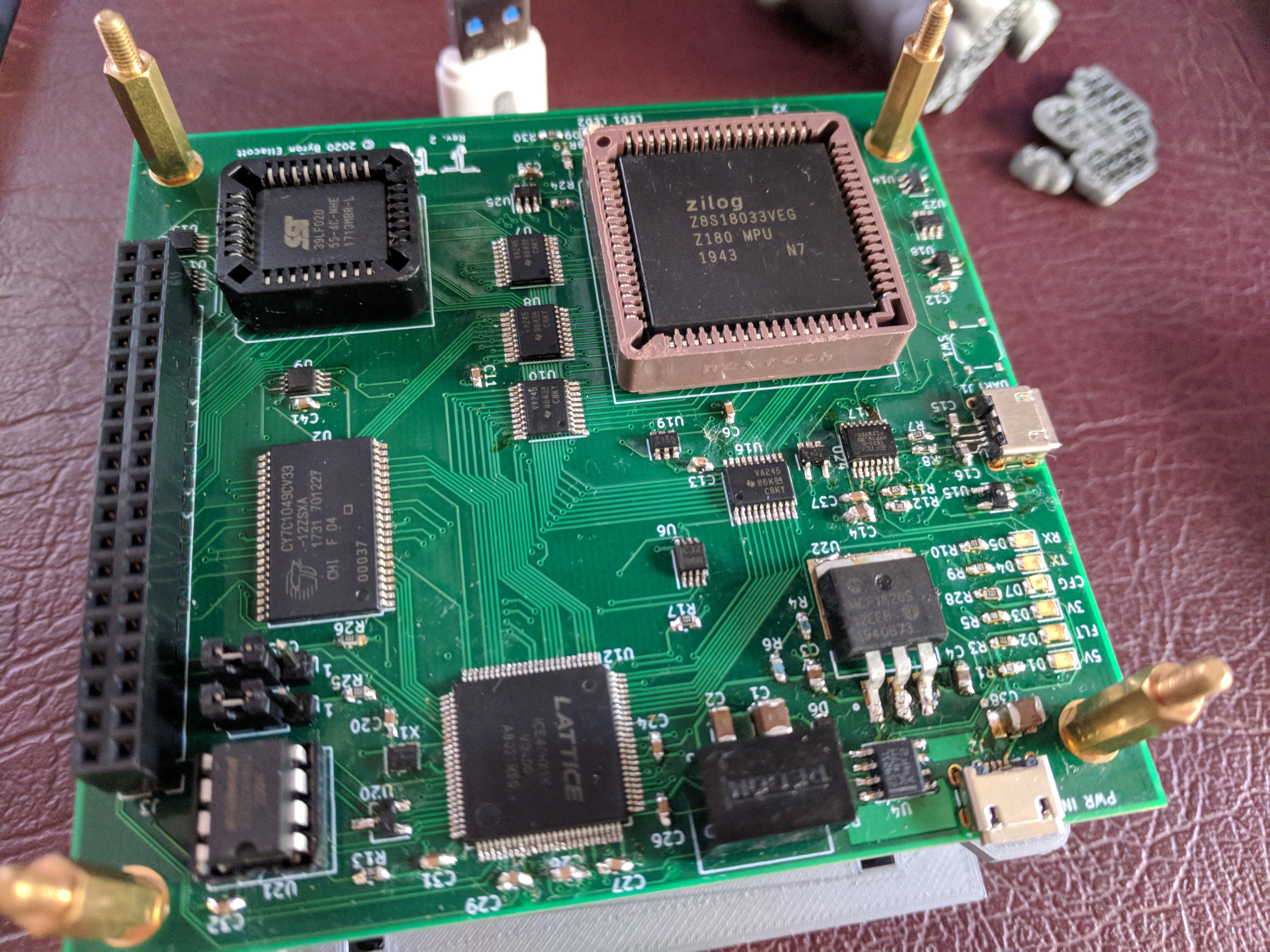
Of course, the job is not really done. Most of the board’s parts aren’t soldered on, and while it’s great that the FPGA works I’ve still yet to get the CPU on. Not to mention all the supporting chips. Time to break out the heat gun and get on with the task.
I put on the FT230X USB IC first, plus its supporting connector and passives. This is for two reasons: I can program the GPIOs on it to ensure the correct VBus sense function and LED output, and because this is the last checkpoint beore I solder on every other part. This worked out fine - the device enumerates correctly, programs fine, and the RX LED flickers in time to keystrokes via USB serial.

Soldering everything else took a few evenings. My process was to squeeze a blob of solder paste onto the DDPAK tab copper area on a board with a bad FPGA solder job, align the target IC with its pads, then use a toothpick to place a sparing amount of paste on the pins. The heat gun then melts the paste onto the pins, and any faults are touched up with the iron.
The best result was the SRAM. It’s possible there’s not quite enough solder on these pins, but I tested every one - I actually found two cold solder joints on the FPGA during this process - and I’m confident they’re all wetted properly.
The worst result was the 18.432MHz oscillator. I underestimated the difficulty of this job, and wound up with far too much solder on it. Solder from the NC pad reached the ground-connected case, and removing it was difficult. I do not feel confident that this part is healthy now.
Install a ROM
The trouble with having finished the soldering is that I don’t much want to blindly power up. The ROM should contain FF endlessly, which will result in the CPU executing RST $38 forever, but it’d be nice to be able to verify in some way that everything’s working as it should. This takes me back to writing a ROM again, but this time for the CPU.
So I wrote a ROM image that sets up ASCI0 to 38400 baud, 8n1, and starts transmitting single character “printf debugging” style progress markers. The only things I do first are to disable DRAM refresh, disable external interrupts, and set the clock rate to the full oscillator speed.
After that, the boot ROM attempts to copy ROM into RAM, reset the ROM overlay D flip-flop, configure the MMU, set up a 100Hz timer, set up a stack, then run a very simple boot monitor that permits a binary to be uploaded using ymodem and executed.
Because I really don’t want to yank the PLCC-32 ROM chip in and out frequently, I don’t want too many rounds of corrections. My emulator is therefore developing more or less in lockstep with the needs of the boot ROM so that I at least have to implement the same bug twice in more or less the same way to miss it. This is a feat I have accomplished in the past, and it’s surprisingly easy to do.
I burned the ROM, plugged it into the board, and with bated breath powered the board up. Good news: the FLT light doesn’t immediately go on, so there’s no major short circuit anywhere. The FPGA still blinks its LED, and the rest sits there, reminding me that I didn’t design in an obvious indicator of CPU health.
I plugged the USART USB cable in, and …

… used some adult language.
Debugging a USB IC
Nothing felt warm. The FLT light was still off. The FPGA was still blinking its LED, now looking more like a taunt than a sign of success.
I busted out the multimeter and did a bit of a probe around, carefully - there’s 3V3 and GND pins right next to each other on the FT230X - only to see all the expected levels. The reset supervisor is not touching /RESET, so it is pulled high by a resistor. The USB cable is delivering ~5V to the voltage divider network. With power removed, I rechecked everything for good solder joints or shorts - everything seems fine.
At a loss, I thought I may as well also test whether the CPU is at least clocking along, so I ran a logic analyser on PHI (and /RESET, to verify the supervisor at the logic level) - and saw only a flat line. The clock was not ticking. It turns out the oscillator just isn’t at all happy, and is not generating any signals. It may still have a short, it may just be toast, either way it’s gotta come off.
I’ve never had much luck desoldering through-hole parts. Solder wick takes a lot of heat to work, and isn’t great even then. My solder sucker was bundled with a cheap soldering iron, and was broken on arrival. I never replaced it. So with a bit of concern that it’d go wrong, I put some heatproof tape on the CPU’s socket and got to work with the heat gun.
To my surprise, I removed the oscillator quite easily. I figured I may as well also remove the FT230X - and this also went far better than I anticipated. Well enough, in fact, that I soldered the removed IC onto a TSSOP-16 breakout board. I replicated the CPU board’s USB circuitry fairly closely on a breadboard, then plugged it in.
The chip is (I think) fine. I can dump its ROM, and I can make an LED flicker by sending to it using the virtual COM port driver.
So I rechecked the CPU board. I checked all the connections into the CPU, which are the only parts I didn’t replicate on the breadboard. I checked all the passives, in case I had a dud resistor or capacitor. Everything looked fine - so, not having much to lose here, I desoldered the poor IC from the breakout board and resoldered it to the CPU board.
Well, that’s it. I can’t communicate with the CPU, I can’t see if it’s working, I’ve no idea what I could possibly do. I am unwilling to risk the price of another board assembly when there’s no apparent reason for failure.
I packed everything away, and nearly didn’t even write this post.
The next day
The only substantive difference between the breadboard setup and the CPU board setup is my admittedly less than perfect USB socket. So after sulkingsleeping on it I tried measuring voltage levels on the breadboard vs. on the CPU board. I ran the USB socket without the main USB power applied to the board: this in theory is perfectly fine, as the FT230X tolerances are absolute, not expressed in terms of its supply voltage. But what I noticed was that VBUS was running at 2V, and D- at -0.5V, relative to ground supplied via the data USB. I checked an unconnected USB socket and got 5V and 0V respectively, with D+ at 3.3V. Hmm.
I reconnected the supply power for the CPU board, and re-measured. Now I saw 5V, 3.3V, and 0V for VBus, D+, and D-, which seemed right. At a loss, I tried one last thing:
It was enumerating again.
This should feel like a victory, but in truth it does not. I don’t know why it didn’t work, I don’t know why it started working, I don’t know whether it will stop working again in the future. But I ordered a replacement oscillator, and may as well press on.